Packaging and Hybrid Integration
‘Breaking the packaging cost barrier’
The Packaging and Hybrid Integration theme focuses on addressing the high costs associated with photonic packaging, which can make up to 80% of the total product cost in certain applications. This cost barrier has limited the widespread adoption of photonics technologies to a few key mass and niche markets, despite their immense potential value.
Research within the IPIC Packaging Theme is centered on developing materials, processes, and technologies that can lower the cost of assembling and packaging photonic devices. The ultimate objective is to transition from current state-of-the-art methods of packaging singulated photonic-integrated chips (PICs) to wafer-level approaches, akin to the gold standard in the electronic industry. These advancements will facilitate surface-mounted and pluggable solutions across various photonic-enabled markets, ranging from telecommunications to LIDAR and biomedical applications.
Research Topics
Package level Thermo-Electric Coolers for thermal management of the photonic integrated circuits
Area: Material Science, Thermodynamics, Wafer-Level Processing
Today, the demand for advanced integration between electronics and photonics within System-in-Package (SiP) architectures requires a dense arrangement of electronic and photonic elements, which poses significant thermal challenges. While electronics typically operate effectively across a broad temperature range, many photonic devices are temperature-sensitive, leading to reduced efficiency in elements like lasers as temperatures rise. Moreover, precise temperature control is essential for certain passive components on the PIC, such as ring resonators.
Currently, achieving this control involves using local heat sources like resistors, with cooling provided by large thermo-electric coolers (TECs) positioned beneath the PIC, cooling the entire chip. However, this setup often increases operational costs significantly.
IPIC’s research focuses on integrating micro-scale thermoelectric coolers to offer localized heating and cooling capabilities for active or passive on-PIC components. Additionally, there is a strong emphasis on developing thermoelectric materials to enhance the efficiency of these cooler devices, ultimately optimizing their performance.
Micro-scale thermoelectric coolers (micro-TECs) rely on growing thermoelectric materials directly onto silicon, leveraging materials with a non-zero Seebeck coefficient. These materials can then be integrated directly onto the device or prepared separately and flip-chipped onto the wafer. Efforts in this area also include enhancing the efficiency of micro-TECs, particularly focusing on improving the efficiency of both p and n-type materials, as their cooling power is closely tied to the efficiency of these thermoelectric materials.
An alternative approach pursued by IPIC for thermal management involves the use of Through Glass Vias (TGVs) as pillars for thermo-electric cooling, termed Substrate integrated micro-TEC (SimTEC). This method entails filling the vias with copper and thermoelectric materials through electroplating, effectively eliminating the additional fabrication costs associated with traditional micro-TECs. SimTEC also provides designers with greater flexibility in customizing substrate thermal design.
The adoption of SimTEC not only leverages the beneficial properties of glass in packaging but also enables targeted and precise thermal management of photonic chips. It enhances thermal connectivity with the surface of the photonic chip while maintaining a compact form factor for the glass package. Consequently, SimTEC presents an attractive thermal management solution for next-generation highly integrated electronic-photonic packaged systems, combining efficiency with design flexibility and cost-effectiveness.
Latest publications
S. Lal, D. Gautam and K. M. Razeeb, Fabrication of micro-thermoelectric devices for power generation and the thermal management of photonic devices, J. Micromech. Microeng. 29, 065015, 2019.
Amit Tanwar, Rajvinder Kaur, N Padmanathan, Kafil M Razeeb, Electrodeposited CuSbTe thin films with enhanced thermoelectric performance, Sustainable Energy Fuels, 7, 4160-4171, 2023.
Rajvinder Kaur, Amit Tanwar, N. Padmanathan, Kafil M. Razeeb, Development of Micro-Thermoelectric Cooler for Thermal Management of Integrated Photonic Sensors, APSCON 2023, Bengaluru, India, 23-25 January 2023.
Parnika Gupta, Amit Tanwar, Xiuyun He, Kamil Gradkowski, Kafil M. Razeeb, Padraic E. Morrissey, Peter O’Brien, Substrate integrated micro-thermoelectric coolers in glass substrate for next-generation photonic packages, Journal of Optical Microsystems, 4(1), 011006, 2024.
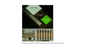
Glass Interposers for Wafer-Level Packaging
Area: Material Science, Thermodynamics, Surface-Mounted Photonics
Glass has emerged as an ideal material for electronic and photonics packaging, especially when compared to silicon. Its advantageous features address traditional packaging challenges, from thermal management to advanced integration and scalable manufacturing. Glass, as a thermal isolator, contains heat at its source, preventing it from spreading to temperature-sensitive components like PICs. However, this property also presents challenges for efficient cooling of devices to maintain stable operating temperatures.
Nevertheless, glass offers the unique advantage of easy via etching, allowing these channels to be filled with metal for thermal conduction and electrical interconnects. This embedded metal not only aids in electrical transmission but also plays a critical role in managing heat, making glass interposers highly promising for integrating photonic packages. Furthermore, glass’s scalability in manufacturing processes promises cost-effective production on a large scale, moving beyond traditional wafer-scale methods.
Addressing these advantages, IPIC’s research focuses on developing high-speed electrical transmission capabilities within glass interposers, optimizing assembly processes for Electronic Integrated Circuits (EICs) and PICs on glass substrates, and establishing design rules for thermal management in glass interposers. This work aims to facilitate manufacturing and standardization in photonics-electronics packaging, driving innovation in this field.
Latest publications
Bernson, Robert, Wakeel, Saif, Gupta, Parnika, Ranno, Luigi, Weninger, Drew, Agarwal, Anuradha, Serna, Samuel, Hu, Juejun, Gradkowski, Kamil, Kimerling, Lionel, O’ Brien, Peter, “Packaging strategies for Photonic and Electronic chips on a Glass substrate.” Electronics Packaging Technology Conference (EPTC), 2023.
Parnika Gupta, Robert Bernson, Noreen Nudds, Sean Collins, Kamil Gradkowski, Padraic E. Morrissey, Peter O’ Brien, “Reference Thermal Chips for 2D and 3D Co-packaging Process Development,” 2023 IEEE 73rd Electronic Components and Technology Conference (ECTC), Orlando, FL, USA, 2023, pp. 2160-2165, doi: 10.1109/ECTC51909.2023.00372.
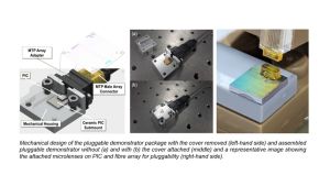
Pluggable photonic packaging utilizing micro-lenses
Area: Optics, Surface-Mounted Photonics, Pluggable Photonic Devices
Traditional photonic packaging involves attaching fibers or fiber arrays to photonic chips to enable optical I/O. However, this process is highly precise, labor-intensive, and challenging to scale, leading to increased costs for packaged photonic devices. To keep pace with the electronic revolution, photonics must transition to pick-and-place surface-mounting techniques that have been perfected in the electronics industry over decades. This shift will not only streamline manufacturing processes but also enhance scalability and reduce costs, making photonics more accessible and competitive in various applications.
One strategy to tackle the challenges mentioned above is to replace the permanent connection between the PIC and fiber with a pluggable one. This approach allows for the photonic chip to be inserted into the package separately, with the optical fiber connection established afterward. This method is especially advantageous in photonics packaging as it simplifies the packaging process, resulting in quicker turnaround times and reduced costs, making it highly appealing across various applications.
In light of this, IPIC’s research focuses on micro-optic arrays at the optical interface, encompassing their design through to system integration, to enable efficient and scalable pluggable connections. Integrating micro-optics helps relax alignment tolerances by enlarging the beam waist and collimating it, making manufacturing more cost-effective. Increasing tolerances by a factor of 5-10 brings packaging within the realm of affordable machining techniques capable of accommodating pluggable connections.
To achieve this goal, the research theme emphasizes designing micro-optic arrays compatible with existing PIC couplers, devising innovative methods for aligning and attaching microlenses to PICs (such as micro-transfer printing for wafer-level attachment or optimizing microlens alignment), and exploring micro-optic materials suitable for diverse application areas and scalable fabrication methods. These efforts aim to advance pluggable connections in photonics packaging, fostering efficiency, scalability, and cost-effectiveness in the industry.
Latest publications
Kamil Gradkowski, David Stegall, David Mackey, Alan Naughton, Terry Smith, Peter O’Brien, “Demonstration of a Single-Mode Expanded-Beam Connectorized Module for Photonic Integrated Circuits”, J. Lightwave Techn. (2023) DOI: 10.1109/JLT.2023.3239138
Luigi Ranno, Parnika Gupta, Kamil Gradkowski, Robert Bernson, Drew Weninger, Samuel Serna, Anuradha Murthy Agrawal, Lionel Kimerling, Juenjun Hu, Peter O’Brien “Integrated Photonics Packaging: Challenges and Opportunities”, ACS Photonics 9(11), 3467, 2022.
Wakeel, Saif, Padraic E. Morrisey, Muhammet Genc, Prasanna Ramaswamy, Robert Bernson, Kamil Gradkowski, Brian Corbett, and Peter O’Brien. “Micro-transfer printing of thick optical components using a tether-free UV-curable approach.” Journal of Optical Microsystems 4, no. 1 (2024): 011003-011003.
Wakeel, Saif, Padraic E. Morrisey, Kamil Gradkowski, and Peter O’Brien. “Through Silicon Optical Coupling for Future Wafer Level Packaging Applications.” Photonics Ireland Conference-2023.
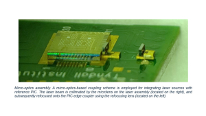
Hybrid integration of lasers
Hybrid integration of lasers poses challenges due to the significant lattice mismatch and differing thermal expansion coefficients between silicon and III-V materials crucial for lasers. As a result, integrating lasers directly onto silicon remains a complex area undergoing active research and development. Several methods have been explored for hybrid integration, such as flip-chip bonding, adhesive bonding, and transfer printing. However, these methods often encounter issues such as low coupling efficiencies or high fabrication costs.
To address these challenges, researchers have turned to microlenses, which play a crucial role in enhancing the efficiency of coupling between optical components. These microlenses not only enable more efficient coupling but also contribute to improved overall performance in integrated photonic devices, making them an essential component in advancing hybrid laser integration with silicon-based circuits.
Within this theme, IPIC’s research concentrates on innovating methods for hybrid integration of lasers onto PICs using microlenses. These methods include direct laser assembly onto the PIC facet or laser sub-assembly, which could take the form of a micro-optical bench within the package substrate. Our solutions show significant promise for efficient laser integration with improved efficiency compared to other techniques, paving the way for further advancements and enabling novel concepts like free-space lab-on-chip technologies.